

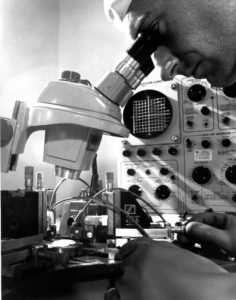
IC Chip Imaging Collecting System
IC chip imaging collecting system include microscope, CCD camera, step-in platform and computer. Microscope is the core of IC chip imaging collecting systems, its imaging quality will determine the quality of whole system. The most commonly known microscope for IC chip imaging collecting includes optical microscope, ultraviolet microscope and scanning electronic microscope.
IC Chip Imaging Collecting System
Optical microscope has tremendous brands to choose, in the field of semiconductor, the mainly used brands have Zeiss, Leica, Nikon and Olympus. Optical microscope is by taking the advantage of visible light to shoot the IC chip imaging, its theoretical limitation is 0.20-0.30um, but in practice, relative better optical microscope can clearly observed the minimum 0.25um.
Ultraviolet or Deep ultraviolet microscope has higher resolution ratio compare with optical light microscope, its theoretical resolution is 97um, in practice, ultraviolet ( deep ultraviolet ) microscope normally apply on IC chip schematic extraction with 0.13um or above. ultraviolet ( deep ultraviolet ) can integrate with optical microscope and use the same microscope framework and lens system, it has one more laser emitting resource, a ultraviolet ( deep ultraviolet ) object lens and ultraviolet ( deep ultraviolet ) CCD camera.
Scanning electronic microscope has 2nd time electron and back scattering electron, 2 kinds of imaging. Scanning electronic microscope’s extreme resolution is 0.2nm, in practice it will mainly being applied on observed and shoot object with 10nm or above, smaller size object will normally choose transmission electron microscope to detect. Due to the most advanced IC chip production line’s capability is 32nm, so for IC chip imaging, scanning electron microscope is sufficient to carry out the task.
Circuit Engineering Co., Ltd can use delayer, coloration technologies to extract IC circuit diagram in each different layers, combine with optical microscopy or scanning electron microscopy to take IC chip photographic (imaging) of each layer with high resolution pictures. In order to better satisfy the customer requirement on pictures viewing, we can provide 3-dimension montage service, and achieve the level of no-cracking on pictures from same layer and preciseness on different layer to realize the 3 dimension whole scene imaging.
Please view below the magnification ration of microscopy for your reference:
| Magnification Ratio (times) | Type of Microscopy | Suitable Line Width |
| 100 | Optical Microscopy | >10um |
| 200 | Optical Microscopy | >3um |
| 400 | Optical Microscopy | 1-3um |
| 1000 | Optical Microscopy | 0.5-1um |
| 2000 | Optical Microscopy | 0.25-0.35um |
| 3000 | Scanning Electron Microscopy | 130-180nm |
| 5000 | Scanning Electron Microscopy | 90-110nm |
| 10000 | Scanning Electron Microscopy | 45-65nm |
Tags: electronic component imaging,ic chip imaging service,ic chip imaging techniques,mcu imaging,microcontroller imaging,microelectronic imaging,semiconductor imaging