

PCB Reverse Engineering Electronic Analysis
In the lifecycle of electronic products, Printed Circuit Boards (PCBs) are the heart of every device. Over time, as systems become obsolete or phased out, their documentation—including Gerber files, schematic diagrams, layout drawings, BOM lists, and netlists—may become unavailable. When a repair, reproduction, or upgrade is needed, companies and engineers often turn to PCB Reverse Engineering Electronic Analysis to recover, restore, or recreate essential design data.
What Is PCB Reverse Engineering Electronic Analysis?
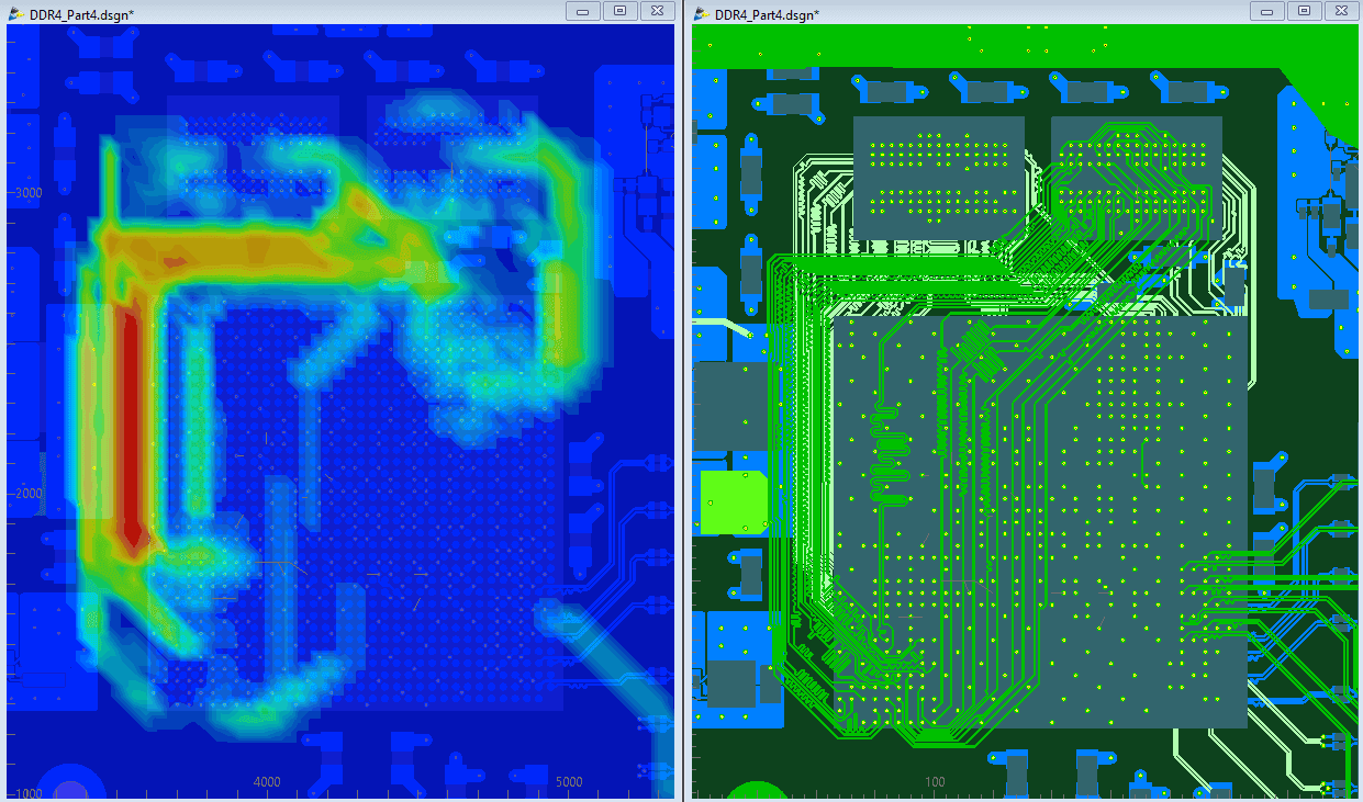
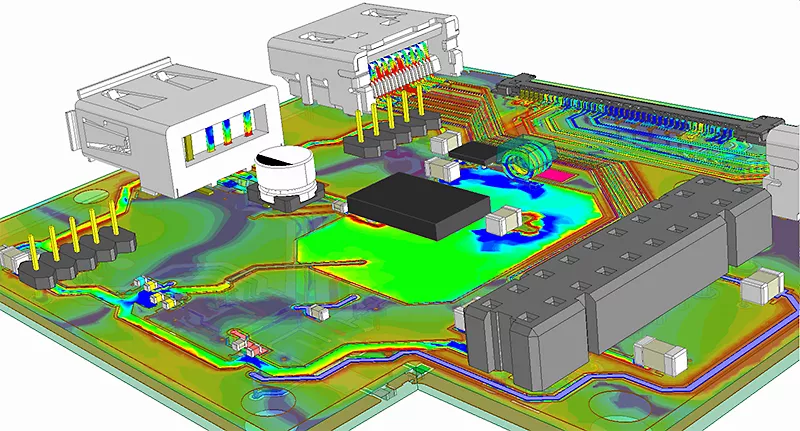
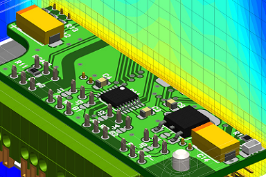
At its core, electronic analysis in PCB reverse engineering refers to the meticulous examination and interpretation of the electrical functions and design logic within a physical PCB. This process goes far beyond visually mapping trace paths or identifying components. It includes signal flow analysis, functional logic tracing, voltage measurements, and sometimes even circuit simulation—all to understand how the board operates and why it was designed the way it was.
This detailed insight is crucial when attempting to recreate, duplicate, or remanufacture a board without access to original source files. For companies dealing with phase-out card PCBs, electronic analysis becomes a gateway to preserving valuable intellectual property and extending the life of critical hardware.
Why Electronic Analysis Is Essential
During the reverse engineering process, simply extracting trace data or copying physical layouts may not be enough. Without understanding the electrical behavior of the circuit—especially in mixed-signal, analog, or high-frequency designs—efforts to replicate the board may lead to failure.
Here’s what electronic analysis enables during PCB reverse engineering:
- Identification of key signal paths and circuit functionalities
- Reconstruction of missing or undocumented schematic diagrams
- Verification of power distribution, ground planes, and decoupling strategies
- Analysis of programmable devices and embedded logic
- Confirmation of netlist accuracy for simulation and validation
- Guidance for redesign or refurbishment of outdated systems
By applying electronic analysis, we don’t just copy a PCB—we understand and reproduce it with precision and confidence.
Application Across Industries
From industrial automation systems to aerospace, medical equipment, and defense electronics, PCB Reverse Engineering Electronic Analysis is increasingly in demand. In the context of redevelopment or redesign of mission-critical electronics, it ensures no part of the reverse engineering process is left to guesswork.
For example, a client needing to refurbish a discontinued motor controller PCB can benefit immensely from this method. Through voltage probing, timing analysis, and digital signal tracing, we’re able to restore the board’s logic and generate a working BOM list, Gerber file, and layout drawing ready for manufacturing.
Empowering Individuals and Companies
Whether you’re a small repair shop, a large OEM, or an individual maintaining vintage electronics, this service bridges the gap between obsolete hardware and modern requirements. Instead of scrapping valuable systems, PCB Reverse Engineering Electronic Analysis gives you a sustainable path to remanufacture, recreate, and even upgrade legacy boards.
Conclusion
Electronic analysis transforms the reverse engineering process from mechanical reproduction to intelligent reconstruction. By leveraging the power of PCB Reverse Engineering Electronic Analysis, companies and individuals can recover lost design data, reproduce legacy PCBs, and revive products once thought impossible to support—all while gaining a deep understanding of the circuitry that makes modern technology possible.