

Electronic PCB Card Cloning Steps
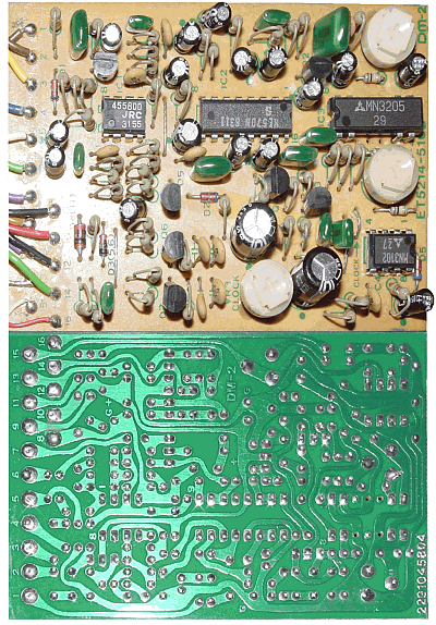
Electronic PCB Card Cloning Steps will be varied depends on the layer count of the Printed circuit board, normally start from desolder the components off target and remove the solder resist layer from copper pattern;
First of all, engineers should layout the various systematic specification on the electronic device, which include the system functions, cost limitation, size and operation situation, etc.
The second step is compile the functional block diagram, also the relationships among these blocks must be layout.
Cut off the Electronic pcb card into several different blocks, can not only decrease the size of Electronic pcb card cloning, but also enable the system with the capability of self-upgrade and component exchange ability.
Systematic block drawing can provide us the evidence and support of separation after Electronic circuit board reverse engineering. For example, the Electronic pcb card from computer can be divided into mainboard, display board, audio board, soft flopy driver and power supply, etc.
Decide the footprint of each components on the PCB board and its dimension after pcb card cloning, after all of the applied technology and circuit quantity have been decided on the Electronic pcb card, the upcoming step is the decision of Electronic pcb card dimension. If the Electronic PCB Board has over its dimension, then we need to change the footprint of it, or relocate the separation action. In the selection of technologies, both the schematic diagram and transmitting speed must be taken into consideration.
Tags: pcb assemble reverse engineering,pcb board reverse engineering,pcb card reverse engineering,pcb reverse engineering,pcba reverse engineering,Printed Circuit Board Reverse Engineering,printed wiring board reverse engineering,pwb reverse engineering,pwba reverse engineering