

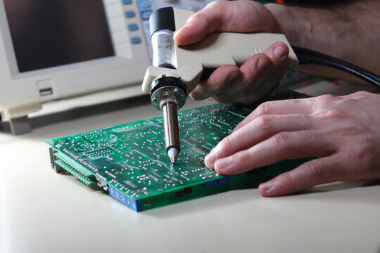
Electronic PCB Board Reverse Engineering Critical Signal
Electronic PCB Board Reverse Engineering Critical Signal refers to the schematic diagram modification especially for printed circuit board applied over the high speed signal transmission field, reverse engineering circuit board schematic will help us to find this critical signal source and termination;
As for the Electronic pcb board reverse engineering, after the thoroughly consideration and prediction, it is preferable to proceed the in circuit test in the preliminary stage of it, and make it become practice in the later stage of electronic pcb board fabrication. And the through hole fan type can be determined by the layout route and in-circuit test, anyway, the power supply and grounding will also affect the layout and spraying.
In order to reduce the impedance value generated by the wave filter capacitor connecting circuit, the through holes must close to the leads of surface mount device as much as possible.
And it is feasible to use the manual layout when necessary, which can have impact on the original designed Electronic pcb display adjustment, it can even cause the re-considering of which through hole is applicable, as a result of that, it is inevitable to consider the relationships between the through hole and lead’s impedance and then define the priority of each through hole.
Manual layout and processing of key signal
Whatever the critical signals quantity, it is first need to layout these signal lines by the schematic diagram provided by PCB reverse engineering, and manual layout or combine with automatic layout are all ok. And the critical signals will achieve the expected performance usually require the dedicate circuit design.
After the completion of printed circuit board schematic diagram, and engineers will inspect these signal lines which become a relatively easier procedures. Through the inspection can fix these lines and then start to draw other signal lines.
Tags: reverse engineering circuit board,reverse engineering circuit card,reverse engineering pcb,reverse engineering pcb assemble,reverse engineering pcb board,reverse engineering pcb card,reverse engineering pcba,reverse engineering printed circuit board,reverse engineering printed wiring board,reverse engineering pwb,reverse engineering pwba