

PCB Reverse Engineering Dimension Analysis
In the world of PCB reverse engineering, precision is everything. Among the many steps involved—circuit tracing, layer mapping, and Gerber file reconstruction—dimension analysis stands out as a critical stage that directly determines the accuracy and usability of the restored board. When we talk about PCB Reverse Engineering Dimension Analysis, we mean a systematic process of verifying, measuring, and adjusting the physical dimensions of a PCB to ensure that the reproduced version matches the original in every mechanical and functional aspect.
Why Dimension Analysis is Essential
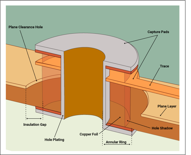
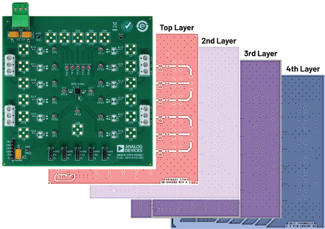
A PCB is not just an electrical circuit—it’s a physical component that must fit perfectly within the product’s housing, connectors, and mechanical interfaces. Even a slight mismatch in board length, width, thickness, or hole position can render a cloned PCB useless. During reverse engineering, our team uses high-precision measurement tools and 3D scanning to recover exact size data. This ensures that the layout drawings, netlists, and schematic diagrams we produce are aligned with the physical reality of the original board.
Dimension analysis is especially vital for products with custom enclosures, such as:
- Industrial control systems
- Medical diagnostic devices
- Aerospace instrumentation
- Consumer electronics with tight packaging
- Automotive control modules
Without accurate dimension data, remanufacture, redevelopment, or refurbishment becomes risky and costly.
The Role of Documentation in Phase-Out PCB Boards
When a phase-out PCB board loses its original BOM list, Gerber file, or layout drawing, companies face significant challenges in repairs, upgrades, or production continuity. Through PCB Reverse Engineering Dimension Analysis, we not only recreate the electrical schematic but also restore the board’s exact form factor. This allows manufacturers to replicate or duplicate a design with confidence, ensuring it will integrate seamlessly into existing assemblies.
By combining dimension analysis with reverse engineering, our services help companies and individuals restore and recreate the complete documentation set for obsolete or unsupported boards. This includes:
- Dimension-accurate Gerber files for fabrication
- Updated schematic diagrams for troubleshooting
- BOM lists optimized for current component availability
- Correct layout drawings for mechanical fitting
Applications and Benefits
The application of dimension-critical PCB reproduction spans across many industries:
- Security equipment: CCTV boards that must fit existing camera housings
- Telecommunication systems: Network interface boards with precise connector alignment
- Medical devices: Circuit boards designed for compact, sealed enclosures
- Industrial machinery: Control boards mounted on legacy production equipment
- Aerospace and defense: High-reliability boards where space tolerance is minimal
For companies, investing in PCB Reverse Engineering Dimension Analysis brings multiple advantages: reduced downtime, cost savings on replacements, and extended lifecycle of existing products. For individuals and small businesses, it offers the possibility to copy or reproduce custom designs without starting from scratch.
j. If dowel pins are used to align mating parts, the location of the pins at the projected distance should be ensured to assure the fit of those parts.
k. Surface finishes on all mating surfaces should be checked, whether or not a gasket is used.
l. Casting surfaces subject to wear for grain structure variances caused by special casting processes should be examined using chills to “harden” the casting in that particular area.
m. Electrical wire diameters should be measured and insulation type and thickness noted. The length of the wire should be duplicated even if it appears to be excessive. Shortening a wire length could change the electrical characteristics of the end item.
3
A manufacturing process variation can produce some strange numbers for part or assembly dimensions. Unless the dimensions or specifications for the next higher assembly are known, “normalizing” of interface dimensions is not recommended.
4
If possible, dimensional analyses should be performed on not less than two items. The results of each may then be compared to determine the possible existence of manufacturing variances as an aid to establishing tolerances, and to ensure they are identical as the probability of randomly selected items with identical defects is negligible.
5
If possible, it should be determined whether items were manufactured in the same lot and this fact noted accordingly for the producibility study. Parts manufactured in the same lot may have very slight dimensional differences, may not accurately depict the allowable tolerances, and may have identical defects.
Conclusion
In PCB restoration projects, missing or inaccurate dimensional data can derail the entire effort. PCB Reverse Engineering Dimension Analysis bridges that gap, delivering the precision needed for successful remanufacture and redesign. By restoring not just the circuit, but the exact physical form, we ensure that even the most complex phase-out PCB boards can live on—ready for continued service in critical applications.