

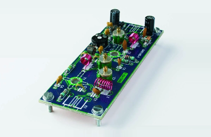
Clone Signal Amplifier PCBA
In the electronics industry, signal amplification is a critical function that appears across countless applications—from industrial control systems to aerospace communication modules, from audio processing equipment to medical devices. When the original designs of these systems become obsolete or the signal amplifier PCBAs (Printed Circuit Board Assemblies) are discontinued, companies are often left with functioning systems they can no longer maintain or reproduce. This is where advanced engineering solutions like Clone Signal Amplifier PCBA services become essential.
What Is a Signal Amplifier PCBA?
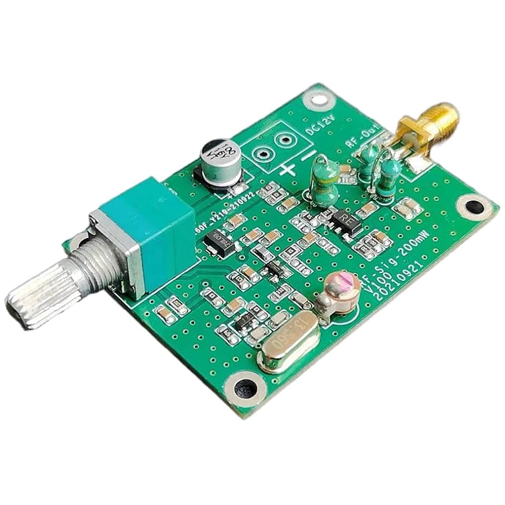
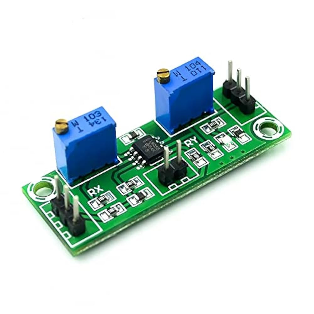
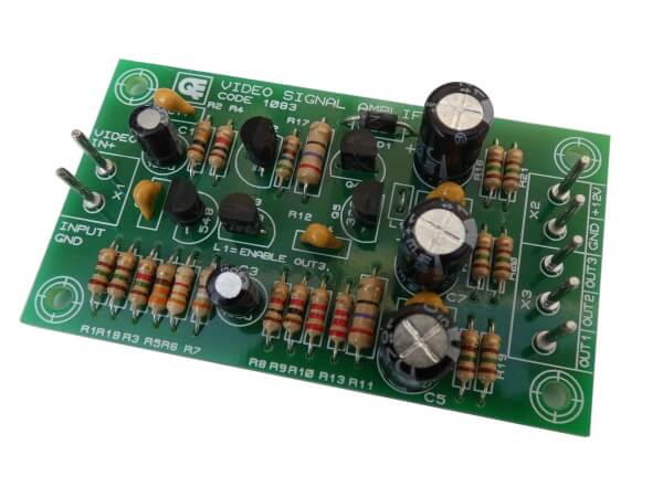
A Signal Amplifier PCBA is a complex board that processes weak analog or digital signals and increases their amplitude for downstream components. These boards often feature precision analog circuitry, operational amplifiers (op-amps), low-noise components, RF shielding, impedance-matched tracks, and heat dissipation design strategies. The layout must consider parasitic elements and noise minimization, especially in high-frequency or high-sensitivity environments.
Typical applications include:
- Audio/visual processing devices
- Wireless communication systems
- Industrial sensors and instrumentation
- Radar and avionics systems
- Medical diagnostic equipment
Because of their sensitivity and critical role in a system’s performance, signal amplifier PCB boards demand exacting engineering and are often designed with strict tolerances.
The Challenges in Cloning Signal Amplifier PCBAs
To clone a signal amplifier PCBA is no simple task. It involves more than just duplicating the visible layers. Successful cloning requires a deep understanding of both analog and digital signal integrity, precise component identification, and careful netlist extraction. Reverse engineers must recover, recreate, and duplicate not only the schematic diagram, but also the layout drawing, Gerber file, and BOM list with full accuracy.
Particular difficulties include:
- Multi-layer PCBs with buried or blind vias
- Precision passive components with no markings
- Custom analog ICs or discontinued parts
- Matched impedance traces and RF layout constraints
- Shielded circuits that hide key sections from surface analysis
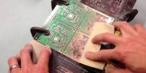
Moreover, amplifiers often include calibration networks or trimming components that influence performance but are not readily evident. Properly reverse engineering and then reproducing these characteristics require specialized tools, such as X-ray inspection, impedance measurement instruments, and high-resolution scanning.
Bringing New Life to Legacy Systems
By opting to clone a signal amplifier PCBA, companies and individuals can restore critical parts of their system that would otherwise be irrecoverable due to manufacturer discontinuation or lost documentation. Our expert services involve every stage of the process:
- Initial data recovery from physical PCBA
- Component desoldering and part mapping
- Circuit tracing and netlist recreation
- High-resolution imaging for layout drawing
- Regeneration of Gerber files and schematic diagrams
- Complete BOM list generation, including modern equivalents
- Prototype remanufacturing and function validation
- Optional refurbish or redesign service to update the board for modern applications
After you get started of your Clone Signal Amplifier PCBA project with us, all the necessary files include Gerber file, layout, BOM and schematic diagram will be submited in below format through which your signal amplifier PCBA can be manufacture and assembly anywhere in the world, we can ensure the accuracy of your data by means of prototype running.
Here is sample of gerber files, schematic diagram and layout drawings acquired base upon our PCB board reverse engineering experience you will receive, based on a typical 4 layers Signal Amplifier PCBA Cloning with components mounted on two sides:
1st Grounding Layer of Signal Amplifier PCBA:

2nd Grounding Layer of Signal Amplifier PCBA:

BOTTOM Layer of Signal Amplifier PCBA:

TOP Layer of Signal Amplifier PCBA:

Schematic Diagram of Signal Amplifier PCBA:

Circuit Engineering Company Limited provide a complete PCB Reverse Engineering, PCB Clone and PCB Restoration service, Rapid Prototyping and functional test services using the latest technologies combined with traditional skills for a wide range of industries. By integrating our traditional skills with the latest technologies, we can offer clients a comprehensive portfolio of product development services all under one roof. For more details please contact our customer
service team.
Conclusion
Whether you need to copy, replicate, or remanufacture a mission-critical amplifier board, our Clone Signal Amplifier PCBA service is designed to deliver highly reliable, engineering-grade results. This service empowers organizations to preserve legacy systems, reduce replacement costs, and regain control over their hardware. It’s not just about duplication—it’s about enabling continued innovation built on proven foundations.