

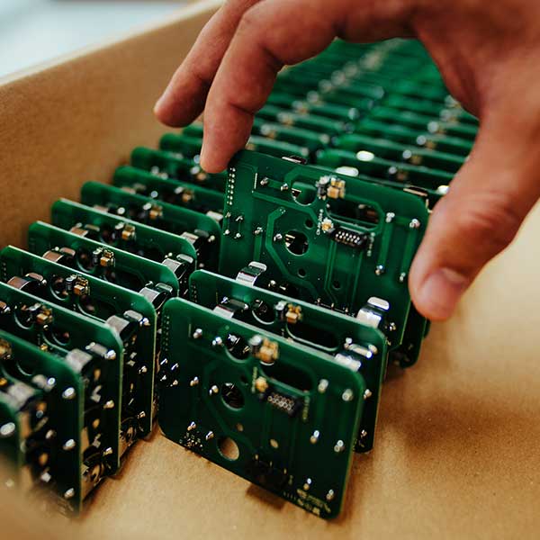
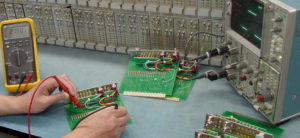
Reverse Engineering Printed Wiring Board
Reverse Engineering Printed Wiring Board can help to acquire the layout drawing, gerber file and schematic diagram out from it, I will show the design of the footprint for a power jack. For through-hole components, make sure that your pads are large enough to manually drill through while allowing enough room for the pins.
I recommend using a pad that has a copper section no less then 80 mils. To ensure this, click on the circle with a 1 in it in the toolbar, as shown in the toolbar figure below. Next, click on the toolbar’s spreadsheet icon shown below. Next, select padstacks, and the pad that you are using should be highlighted. Change the parameters to the following as shown in below figure.
This will now ensure that your pads are large enough to place the pin through, while having enough room to solder the pin. The next step is to follow the specifications on your data sheet and design the footprint for the power jack, footprint can be modified through PCB reverse engineering technique.

The dimensions can be determined from the X,Y coordinates in the top left corner of the Screen. Make sure that you follow the pin out according to the way in which you connected your new layout drawing and Gerber file in Capture obtained from circuit board reverse engineering. To add a new pin, right click your mouse and select new. To place the part, left click. When you are complete making your pads, you must make a place outline around your component. To do this, click on the following icon.
Tags: reverse engineering circuit board,reverse engineering circuit card,reverse engineering pcb,reverse engineering pcb assemble,reverse engineering pcb board,reverse engineering pcb card,reverse engineering pcba,reverse engineering printed circuit board,reverse engineering printed wiring board,reverse engineering pwb,reverse engineering pwba