

Reverse Engineering Printed Circuit Board Polygons
Sometimes it’s useful to fill large areas with solid copper when reverse engineering Printed Circuit Board. The way to do this is with polygons. Polygons can be created in either the polygon mode or the rectangle mode. In the polygon mode, you’ll have to define each corner of the polygon with a mouse click (Btn1 ). When the last point is clicked exactly on top of the starting point, the polygon is finished.
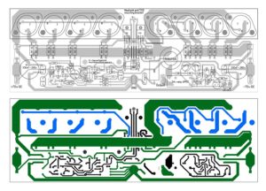
Reverse Engineering Printed Circuit Board needs to delayer the PCB board and desolder all the parts off the board, then copy layer copper pattern
Since this can be hard to do, the Shift-P key will enter the final point for you, closing the polygon. If the 45 degree angle restriction is turned on and you try to close the polygon when it is not possible, you’ll get a warning instead. If you haven’t finished entering a polygon, but want to undo one (or more) of the points that you’ve already defined, use the undo command (U key) for PCB Plate reverse engineering inspection.
With the rectangle tool, defining the two diagonally opposite corners is sufficient, but of course the resulting polygon is a rectangle. Like lines, a polygon can by edited by deleting, inserting and moving the points that define it. Pins and vias always clear through polygons without touching them when first positioned. You must add a thermal with the thermal tool in order to connect pins and vias to polygons. Thermals can be added and removed by clicking Btn1 with the thermal tool over the pin or via.
The thermal tool always places a thermal to polygons on the active layer extracted by PCB card cloning technique, so if the tool doesn’t seem to work, it’s probably because the polygon you want to touch is not on the active layer.
Tags: reverse engineering circuit board,reverse engineering circuit card,reverse engineering pcb,reverse engineering pcb assemble,reverse engineering pcb board,reverse engineering pcb card,reverse engineering pcba,reverse engineering printed circuit board,reverse engineering printed wiring board,reverse engineering pwb,reverse engineering pwba