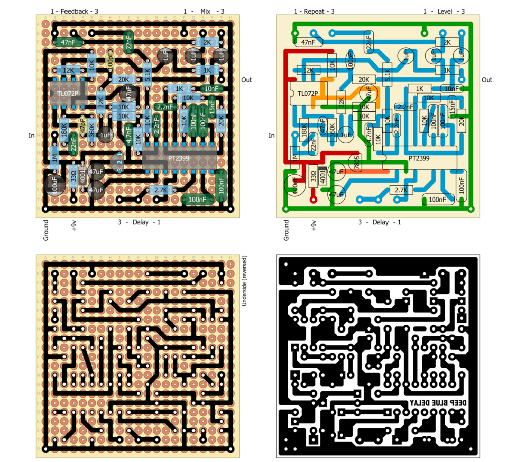
Reverse Engineering PCB Circuit Card Drawing
Reverse Engineering PCB Circuit Card Drawing needs to desolder all the components off the PCB circuit board, and delayer the PCB board from solder mask layer and copper circuitry pattern for scanned images;

1, the orientation of printed circuit board reverse engineering restriction: from view of soldering side, the layout and orientation of components must keep the same orientation with schematic diagram as much as possible, and layout orientation had better keep the same line with schematic circuit layout orientation, since various kind of parameter inspection should be proceed from the soldering side of manufacturing, as a result of that, this way of treatment is easier for the inspection in the production, debugging and repair;
2, each component’s arrangement and layout must be as much of reasonable, and well distributed as possible, with great cosmetic performance and well structure to satisfy the technical requirement to comply with the PCB layout design;
3, the layout methods of resistor and diode has only two ways, vertical or horizontal:
1> Vertical, if the quantity of components is not too much, as well as the dimension of pcb circuit card is not quite big, normally we can place them vertically; as for those resistors with value lower than 1/4 W, the distance between their pads must be 4/10 inch which can be changed through Reverse engineering PCB and optimize its layout, the resistor with 1/2W, distance between their pads is 5/10 inch; for the diodes, 1N400X series rectifying tube, normally need to use 3/10 inch; 1N540X series rectifying tube, use 4 to 5/10 inch.
2> Horizontal, when the quantity of electronic components on the PCB circuit card is big, and the dimension of pcb circuit card is not very big, usually we should use the horizontal method, and the distance between the two soldering pads should be 1 to 2/10 inch.
Tags: replicating circuit board,replicating circuit card,replicating pcb,replicating pcb assemble,replicating pcb board,replicating pcb card,replicating pcba,replicating printed circuit board,replicating printed wiring board,replicating pwb,replicating pwba

