

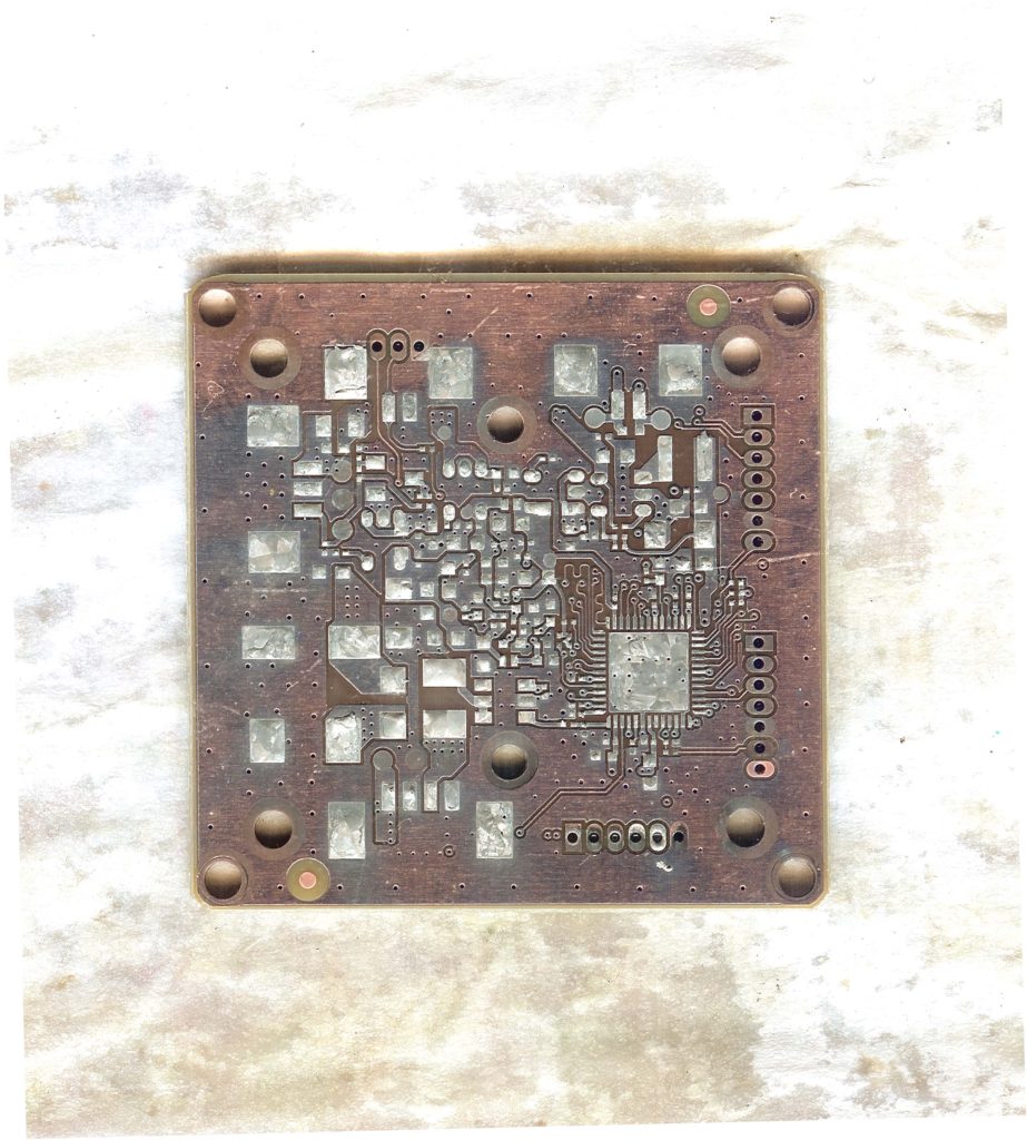
Reverse Engineering PCB Circuit Board Layout
Reverse Engineering PCB Circuit Board Layout can extract circuit diagram from original electronic circuit card which can be used for re-manufacturing;
Automatic layout when reverse engineering printed circuit board digital wiring need to control some electrical parameters especially for these critical signal lines, such as the reduction of dissipated capacitance and EMC, which is also feasible for other signal line layout. All of the EDA manufacturers can provide a way to control these parameters.
After the understanding of the input parameters and their effects on the parameters from automatic layout tools, the quality and stability of automatic layout from Printed circuit board duplicating can be secured.
General rules must be adapted to layout the signal lines automatically. Through the installation of restriction terms and prohibition layout area to limit the used layer from prescribed signals and all of the through holes used, layout tool can optimize printed circuit board according to engineer’s thoughts. If there is no limitation on the through hole quantity and used layers, automatic layout will apply all of the layers and generate too many through holes.
Tags: pcb assemble reverse engineering,pcb board reverse engineering,pcb card reverse engineering,pcb reverse engineering,pcba reverse engineering,Printed Circuit Board Reverse Engineering,printed wiring board reverse engineering,pwb reverse engineering,pwba reverse engineering