

Reverse Engineering PCB Board with Large Area Grounding
Reverse Engineering PCB Board with Large Area Grounding normally apply on the electronic facilities with high power supply and voltage transmission;
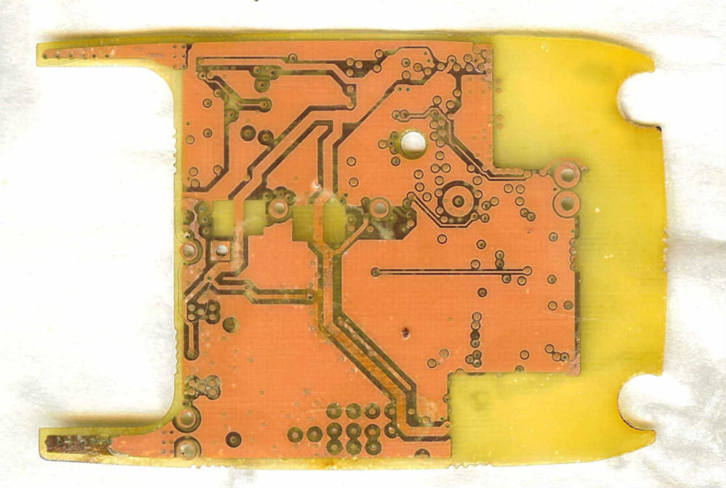
Reverse Engineering printed circuit board with a mixture of Digital/analog circuit design, there could be A/D, D/A, FPGA and source less wave filter, its working frequency can achieve approximately 40M, so there are several aspect in the process of PCB Board circuitry diagram restoration, especially when layout the large area grounding.
Generally speaking, the main purpose of copper grounding with large area is to form the shielding for the electronic magnetic radiation, and there is similar functions for network grid and large copper area, however, if the copper circuit track on the electronic PCB card relayout is extremely thin, then there could be several minor difference between the network grid and copper foil surface, if the circuit track is relatively thick then it is not an issue;
But the network grid design can bring more benefit to the adhesion between the solder resist mask and glass fiber resin material, as a result of that, it is better to consider use the network grid, as for single sided circuit board or double sided electronic PCB restoration, it needs to mainly concern about the impedance affection.
Generally speaking, double sided PCB board Reverse Engineering require no consideration on the impedance control, while in the real scenario, add a symmetrical lines on the two sides of PCB board can also be considered as a shielding method, so engineers should still take cloning PCB card as priority and there would be not big issue.
Tags: duplicate circuit board,duplicate circuit card,duplicate pcb,duplicate pcb assemble,duplicate pcb board,duplicate pcb card,duplicate pcba,duplicate printed circuit board,duplicate printed wiring board,duplicate pwb,duplicate pwba