

Reverse Engineering PCB Board Wiring Diagram
Reverse Engineering PCB Board Wiring Diagram
When Reverse Engineering PCB Board wiring diagram, we need to identify the PCB circuit pattern dissipation and layout PCB circuit pattern logically:
For distinguish of ground plane, power supply circuit and signal circuit, also require engineer to have related power supply, circuit connection, PCB board layout and PCB reverse engineering knowledge. How to distinguish these different kinds of circuit can rely on component connection situation, copper thickness and feature of electronic product.
During the process of PC board layout & Reverse engineering, in order to avoid the cross line, large bulks of ground signal can be applied on the ground plane, different circuit can use different colors to help distinguish one another, also specified symbol can use on specified components, can even separate unit circuit and draw them. And finally can integrate them together.
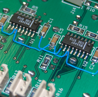
And then Master the basic framework, take the similar wiring diagram after PCB Board reverse engineering as reference:
For those basic formats of electronic PCB circuit and PCB wiring diagram drawing, engineer should understand them very thoroughly, because they can help to draw some simple and typical circuit unit directly, but also form electronic circuit framework.
From other side, please remember that same kind of electronic product can be similar to a certain extent, engineer should accumulate more experience and can take them as reference to reverse engineering other PCB.
5 Checking and Optimization:
Whole process of reverse engineering PCB wiring diagram finish only after checking and testing done and approve pass, for nominal value of those distribution parameter sensitive components of PCB need to check and optimizing, according to PCB design or PCB reverse engineering process, compare the PCB wiring diagram with design file to ensure the accuracy and completeness.
Tags: reverse engineering circuit diagram,reverse engineering schematic diagram,reverse engineering wiring schematic