

Reverse Engineering PCB Board Schematic Design for Mixed Signals in Separated Area
Reverse Engineering PCB Board Schematic Design for Mixed Signals in Separated Area can help to improve the performance of electronic-magnetic interference resistance, through relayout circuitry scheme the PCB circuit board will provide a better and stable performance.
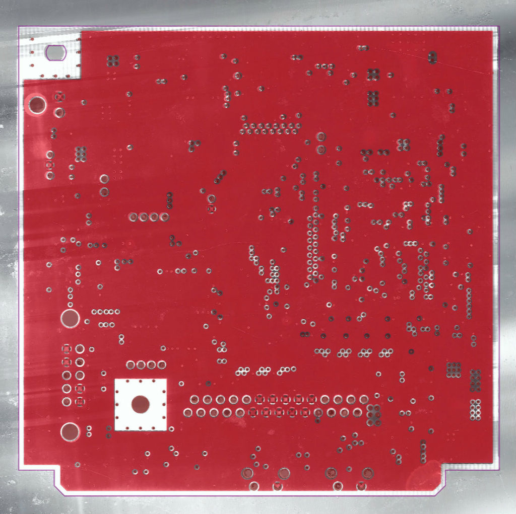
PCB board reverse engineering calibration will refers to the mixed signals issue, especially for the current electronic consuming products, most of them have the mixed signals on the separated area and PCB designer should be aware of this point.
As we all know, PCB board with mixed signal circuit which include digital circuit and analog circuit could be extremely complicate compare with other printed circuit board. The electronic component arrangement, PCB layout as well as the power supply and grounding line treatment can directly affect the electrical performance and electro-magnetic performance.
So the engineers will sufficient experience can optimize the mixed signal PCB board design features through the separation of ground and power supply circuit.
There is one way to solve the issue suggested by PCB Reverse Engineering engineer which is cut off the area and separate the digital ground and analog ground on the mixed signal PCB board, which can help to realize the separation between digital ground and analog ground.
Although this could possibly a feasible way to tackle PCB board Reverse Engineering issue, but it still has the problem of its own, and these problems will emerge in the large complicate system and become more obviously.
And the key point is the separation line couldn’t be cut off or cross, once the separate line being crossed, electronic-magnetic radiation and signal cross talk will increases dramatically. And the most commonly see issue in the PCB board layout is signal line cross the separation line no matter for grounding or power supply, it can generate the ELECTRO-MAGNETIC INTEFERENCE ISSUE.
Tags: reverse engineering circuit board,reverse engineering circuit card,reverse engineering pcb,reverse engineering pcb assemble,reverse engineering pcb board,reverse engineering pcb card,reverse engineering pcba,reverse engineering printed circuit board,reverse engineering printed wiring board,reverse engineering pwb,reverse engineering pwba