

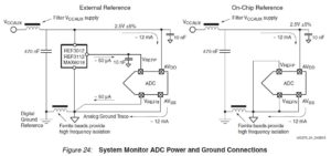
Reverse Engineering PCB Board Analog Ground
Reverse Engineering PCB Board Analog Ground must considering the situation when the high-frequency current flowing through the large loop generates radiation and high ground inductance. If a large-scale analog current flows through the large loop, the current is easily disturbed by external signals.
The worst part is that when the split ground is connected together at the power supply, a very large current loop is formed. In addition, the analog ground and the digital ground are connected together by a long wire to form a dipole antenna.
Understanding the path and manner in which current flows back to ground is key to optimizing mixed-signal board design when Reverse Engineering PCB Board Analog Ground. Many design engineers only consider where the signal current flows, ignoring the specific path of the current.
If the ground layer must be split and must be routed through the gap between the splits, a single point connection can be made between the divided grounds to form a bridge between the two grounds, and then routed through the bridge.
Reverse Engineering PCB Board Analog Ground
In this way, a direct current return path can be provided below each signal line, resulting in a small loop area. Signals can also be used to span the split gap using optically isolated devices or transformers. For the former, the optical signal is crossed across the split gap;
in the case of a transformer, the magnetic field is crossed across the split gap. Another possible solution is to use a differential signal: the signal flows back from one line and returns from the other. In this case, it is not required as a return path.
To delve into the interference of digital signals with analog signals, you must first understand the characteristics of high-frequency currents. The high-frequency current always chooses the minimum impedance (lowest inductance), directly in the path below the signal, so the return current will flow through the adjacent circuit layer, regardless of whether the adjacent layer is the power layer or the ground layer.