

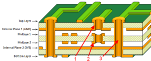
Multilayer PCB Board Vias
Multilayer PCB Board Vias is one of the important components since the cost of drilling is usually 30% to 40% of the cost of PCB board manufacturing. Simply put, every hole in the multilayer PCB board can be called a via and it is critical for electrical integrity of PCB reverse engineering and functionality.
In terms of function, the vias can be divided into two types: one is used as an electrical connection between the layers; the other is used for fixing or positioning the device.
In terms of process, these vias are generally divided into three categories, namely blind vias, buried vias, and through vias. The blind holes are located on the top and bottom surfaces of the printed wiring board and have a depth for the connection of the surface lines and the underlying inner lines, and the depth of the holes usually does not exceed a certain ratio (aperture).
Multilayer PCB Board Vias
Buried hole refers to a connection hole located in the inner layer of the printed wiring board, which does not extend to the surface of the circuit board. The above two types of holes are located in the inner layer of the circuit board, and are completed by a through hole forming process before lamination, and several inner layers may be overlapped during the formation of the Multilayer PCB Board Vias.
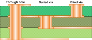
vias in the multilayer PCB board
The third type is called a through hole, and the hole passes through the entire circuit board and can be used to implement internal interconnection or as a mounting hole for the component. Since the vias are easier to implement in the process and lower in cost, most printed circuit boards use it without the need for two other vias. The via holes described below are considered as through holes unless otherwise specified.