

Reverse Engineering Electronic PCB Board Service
Reverse engineering ELECTRONIC PCB BOARD Service has been widely applied on a great variety of industry, as we all know, it still one of the most prevail and normally use Assembly technology in the ELECTRONIC PCB BOARD manufacture: through hole design technology. So in the process of PCB board assembly, we still have a lot of chances to see and need to get used to this kind of technology:
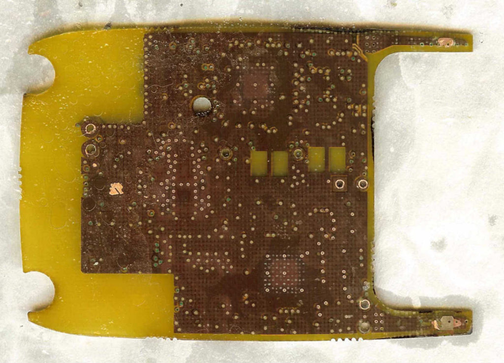
Reverse engineering Electronic circuit board need to strip off the copper pattern layer on it and scanning each one layer of it. After the scanning process done, we need to layout each one of them as one of the most critical part in whole process of electronic pcb board cloning, proper Electronic pcb board layout can save you a lot of troubles:
1; layout all of the circuit track on top of the Electronic pcb board after reverse engineering, since the bottom side (soldering side) could be damaged easier. Don’t layout the circuit track on the edge of PCB, since the edge will usually be hold by the facility and can cause damage;
2; as for those components with more pinouts, such as the cable terminals and flat cable, engineer should choose to use ellipse round instead of round when reverse engineering Electronic pcb board, which can help to prevent the solder tin bridge when wave soldering;
Tags: replicate circuit board,replicate circuit card,replicate pcb,replicate pcba,replicate printed circuit board,replicate printed wiring board,replicate pwb,replicate pwba