

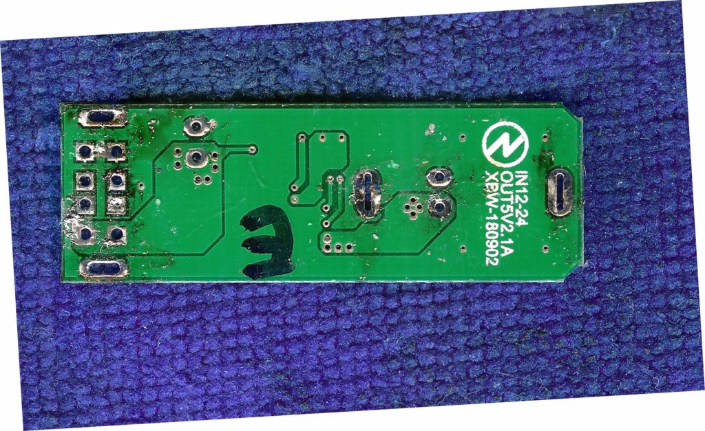
Reverse Engineering Electronic PCB Board Design
Reverse Engineering Electronic PCB Board Design include Layout scheme, schematic drawing, component list and Gerber file, and use these documents to clone printed circuit board;
no matter what kind of Electronic pcb board design software you are about to use, each one of them will have the automatic copper clad functions which has played an important role in the Reverse Engineering Electronic pcb board technology. The necessity of Copper clad process has several reasons:
1; one of the greatest advantages of copper clad is low down the impedance value in the ground line (the majority of grounding impedance was brought by the so call anti-inteference), there are great amount of peak pulse current exist in the digital circuit, as a result of that, it seems more necessary to bring down the impedance from the grounding, it is commonly believe that the Electronic pcb board which constituted by digital circuit parts should have copper clad in great size, as for analog circuit, the grounding revert route generated by copper clad will cause decoupling interference, it is certainly the lost outweight the gain. Consequently, not everyone of the Electronic pcb board will require copper clad when reverse engineering it. By the way, copper clad with network shape has better effect than large area of copper clad.
– relevant power supply, ground, signal and return route must parallel to eliminate the noise;
– keep the clock line, data-bus separated with the input/output line and connectors after printed circuit board reverse engineering;
– Route time clock signal crossing the input/output signal;
– minimize the crosstalk, trace need to use right angle crossing and dissipated ground line from reverse engineering printed circuit board;
– protect the critical trace use 4 mils to 8 mils tracks to miniature the inductance, and ensure the tracks is closely attached to the ground layer, and the interlayer must use the clapping structure to protect each side of the clapping layer from printed circuit board gerber file cloning has contact with grounding;
Wave Filtering Technology
– power supply source and basic voltage lead for side-road analog circuit;
– Swift switch components of sideroad
– decoupling the power supply and ground on the component pin lead;
– use multiple wave filtering to attenuate the multi-level power supply noise;
Tags: replicate circuit board,replicate circuit card,replicate pcb,replicate pcb assemble,replicate pcb board,replicate pcb card,replicate pcba,replicate printed circuit board,replicate printed wiring board,replicate pwb,replicate pwba