

Replicating Printed Circuit Board Gerber File
Replicating Printed Circuit Board gerber file, layout drawing, schematic diagram and BOM, and then use these producible documents to reverse engineering electronic circuit board;
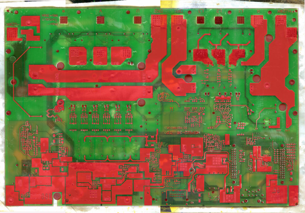
When Replicating printed circuit board, no matter what kind of pcb board design software you are about to use, each one of them will have the automatic copper clad functions which has played an important role to restore schematic diagram from pcb card reverse engineering technology. The necessity of copper clad process has several reasons:
There are three effects:
1; cosmetic performance;
2; depress the noise;
3; decrease the high frequency interference (follow pcb board layout rules);
In view of the high frequency, there are a lot of issues refers to 90 degree, as we know, no engineers who proceed the manual soldering will draw the layout in that way.
If you happen to see there is any occurrence of layout in that way, then it must because there is some surface mounted device on the PCB board. Because there is a technology name wave soldering during which the bottom side of PCB could be overheated partially and cause BOW & TWIST.
Tags: replicate circuit board,replicate circuit card,replicate pcb,replicate pcb assemble,replicate pcb board,replicate pcb card,replicate pcba,replicate printed circuit board,replicate printed wiring board,replicate pwb,replicate pwba