

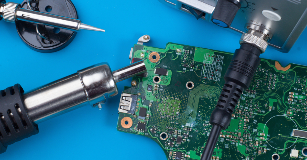
Replicating PCB Circuit Card
When Replicating PCB circuit card, processing the ground bouncing noise and SSO switch noise is a headache issue and people will nornally understand the severerity of these issues. A successful example of PCB Circuit Card Replication will involve a perfect PCB Board Clone through a flawless layout drawing, Bill of Material, Gerber file and Schematic diagram obtained by PCB Reverse Engineering Technique.
In the EDA, this noise will be contributed to the POWER INTEGRITY analysis scope, especially in the high speed pcb circuit card replicating, the unstable working condition is commonly situations, it is quite probably be caused by the switch noise or ground bounce noise. And these issues can be solved by pcb circuit card reverse engineer through some simple ways.
In view of the fixed quantity will be more complicate. For example, a kind of simple SSO switch noise elimination method is adding wave filter capacitor among the ground and power supply layer, and the most commonly used method is add the electros with different quality and types, and engineer with less effort to confirm the maximum voltage of capacitor, it can be calculated by the working voltage of pcb circuit card, but the way to ensure the capacitance of these capacitors are consistently depends on the working experience of pcb circuit card reverse engineer or take other circuit layout as reference.
Since it is quite difficult to calculate the pcb circuit card replicating SI/PI value, especially the current pcb circuit card with much more difficult and complicate design, it is almost impossible to calculate it by bare hand. The location of capacitor is one of the uncertainty issues. But these electros locations and their wave filtering effect must be closed related. By using the APSIM-SPI tools, pcb circuit card reverse engineer can swiftly design and verify the effect of wave filtering. And can confirm their location effectively as well as their values. Abundant capacitance should be disposed stoutly. And the necessary capacitance should be ensured the quantity.
APSIM-SPI also has a lot of other features refers to the signal singularity and simulation design. The high speed pcb circuit card replicating must use advanced affiliated method to proceed, SPI is a tool which combine years of experience and other advanced SI and PI analysis technology, which can be used to simulate the PCB CIRCUIT CARD working condition in a relative real environment which can make the pcb circuit card replicating closer to real test result. SPI provides a completely new debugging platform.
Tags: replicating small pcba artwork,replicating small pcba bom,replicating small pcba cad file,replicating small pcba design,replicating small pcba drawing,replicating small pcba gerber file,replicating small pcba layout,replicating small pcba schematic