

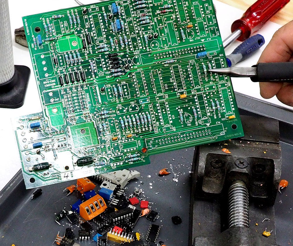
Replicate Multilayer Printed Circuit Board
Replicate Multilayer Printed Circuit Board starts from restore layout scheme, Gerber file, BOM and schematic diagram from existing PC board, and re-manufacture printed circuit board accordingly;
In order to increase the layout size after PCB board reverse engineering schematic diagram, multilayer PC board will require to use more single side and double side PCB. The process will refers to several double sided PCB Board, and place the insulated adhesive film among each one of the double sided PWB and then press them together.
The layer count can represent the the numbers of individual layout layers and normally they are even number which contains the outer layers. In most of the computer mainboard, you will find out that their main structure is 4 to 8 layers, anyway, theoretically speaking we can Reverse engineering PCBA populated card as many as 100 layers. The super main computer in most cases will use multilayer PRINTED CIRCUIT BOARD with more than 20 layers.
However, due to these kind of super computer nowadays can be substituted by a lot of normal computers sets pool, this super multilayer PC board is useless any longer. Since the combination of multilayer PRINTED CIRCUIT BOARD is quite tight, so when copy electronic pcb board gerber file, it is quite difficult to tell their exact layer count, anyway, if you are familiar with the mainboard, it is possible to see through it.
Tags: replicate circuit board,replicate circuit card,replicate pcb,replicate pcb assemble,replicate pcb board,replicate pcb card,replicate pcba,replicate printed circuit board,replicate printed wiring board,replicate pwb,replicate pwba