

Printed Circuit Board Reverse Engineering Measurement Technique
Printed Circuit Board Reverse Engineering Measurement Technique include measured by facilities and by handheld device, for low level negative components like low value capacitors & resistor, inductors a proper multi-meter is good enough, for high level electronic active components such as integrated circuits, transformers, crystal with high frequency, facilities will be required;
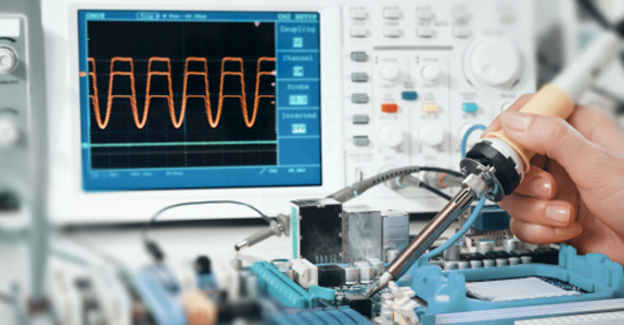
Proper measurement techniques for PC Board Reverse Engineering are essential to obtain accurate PCB characterization results. We would like to describes the techniques required to make accurate probing and data extraction measurements using the TDR, including proper instrument calibration procedures.
General Equipment
The following instruments or equivalents are recommended for PWB Board cloning esd effect:
- · Tektronix 11800 series with SD24 TDR module
Rambus App Note- Appendix A
- · Hewlett-Packard’s HP54750A with HP54754 TDR module
- Rambus App Note- Appendix C
- · Polar Instruments CITS500s
Rambus App Note- Appendix B
Impedance coupon general length recommendations are based upon the instruments that will be used for Measurements
Calibration is essential for ensuring that the equipment being used is measuring correctly after high speed PCB Board Reverse Engineering and with maximum accuracy. This is the first critical procedure necessary to ensure proper instrument setup prior to starting measurements. Proper instrument calibration and verification on a regular basis cannot be over emphasized.
Calibration procedures for each type of equipment should be referenced in the user manual. The following section describes procedures for the Tektronix 11801B Digital Storage Oscilloscope with SD24* sampling head.
Calibration should be performed on a daily basis. After calibration is completed, leave the 50 Ω load termination on the instrument. Turn cursors with TDR vertical scale reading in units of rho and verify that the reading is 50 Ohms.
TDR sampling heads are susceptible to static discharge damage. This damage will not necessarily render the head inoperable but can induce measurement error. The following steps can be completed to check for static damage.
- · Connect the 50 Ω load termination.
- · Adjust the time scale to ~ 500 ns/div
The upper portion of the pulse should be flat without sagging..
A 50 Ω air-dielectric reference load will provide the best accuracy for calibration. Air-dielectric loads can be used to obtain the reference voltage used to calculate load impedances. Air-dielectrics should be used to obtain the highest accuracy (>0.4 Ω) after PCB board cloning.
Tags: pcb assemble reverse engineering,pcb board reverse engineering,pcb card reverse engineering,pcb reverse engineering,pcba reverse engineering,Printed Circuit Board Reverse Engineering,printed wiring board reverse engineering,pwb reverse engineering,pwba reverse engineering