

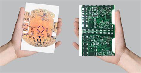
PCB Reverse Engineering Test Structure
PCB Reverse Engineering Test Structure described in this document are intended for determining trace characteristic impedance and propagation velocity.
High-speed bus designs require improved impedance and coupling control to satisfy voltage and timing budgets in the process of Printed Circuit Board duplication. This means careful attention to bus design trace geometry in order to develop proper test coupons. The following sections provide recommendations for improved test coupon designs.
Requirements for Matching Test Coupon to Bus Design
Test structures should allow you to extract impedance and velocity characteristics that represent actual traces in the bus layout from PCB circuit card gerber file replication. To represent the characteristic impedance and the design accurately, test coupons must follow bus layout guidelines, including trace to trace spacing and ground shielding.
Bus designs like the Direct Rambus* channel depart from typical designs of Printed wiring board by operating in pipeline mode to provide data rates up to 800 MT/s. Sensitivity to trace impedance matching and coupling must be minimized to reduce affects like inter symbol interference (ISI). Implementing ground shields or floods between signal traces reduces trace-to-trace parasitic coupling. Improved trace to trace impedance control is achieved by inserting ground shields in between signal lines. This provides a uniform copper density across the bus to ensure etch characteristics are equivalent for all signal lines.
These ground shields also add capacitive coupling to ground which affects the trace characteristic impedance. Test structures without dummy traces or floods will not represent the actual bus characteristic impedance and will also exhibit more etch variation (thus, more Zo variation) in the coupon than the actual bus if PCB card cloning.
Tags: pcb assemble reverse engineering,pcb board reverse engineering,pcb card reverse engineering,pcb reverse engineering,pcba reverse engineering,Printed Circuit Board Reverse Engineering,printed wiring board reverse engineering,pwb reverse engineering,pwba reverse engineering