

PCB Reverse Engineering Rule
PCB Reverse Engineering Rule and limitation MUST be followed, if the PCB board reverse engineering task can be done smoothly, the tools must work in the environment of correct rules and proper limitation.
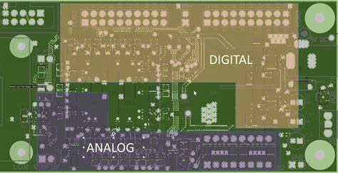
All the signals track with special requirement must be classified, all sorts of signals must have priority level, the higher the priority level, the strict the rule is it. These rules should include PCB track width, through hole maximum quantity, parallel level and interference among these signal tracks and layer count limitation.
These PCB Reverse Engineering rules will play an extremely influence on the PCB card cloning tools and process.
Component Layout
In the pursuit of component assemble optimum, REVERSE ENGINEERING FOR MANUFACTURE rule will have restriction on the component layout. if the PCB assemble department allow to move the component location, the circuit PCB can be optimized advisablely and will make it more convenient for automatic PCB design and layout. Automatically printed wiring board copying will only take one signal into consideration, PCB design tools can complete the layout work like the engineers through the installation of limitation rules and signal layer for design and layout.
Tags: dupliquer pcb bom,dupliquer pcb design,dupliquer pcb layout,dupliquer pcb part list,dupliquer pcb schematic,pcb assemble reverse engineering,pcb board reverse engineering,pcb card reverse engineering,pcb reverse engineering,pcba reverse engineering,Printed Circuit Board Reverse Engineering,printed wiring board reverse engineering,pwb reverse engineering,pwba reverse engineering