

PCB Recovery of 3G Wireless Router
PCB Recovery of 3G Wireless Router
After you get started of your 4 layer PCB Recovery of 3G Wireless Router project with us, all the necessary files will be submited in below format through which your 4 layer Printed Circuit Board can be manufacture and assembly anywhere in the world, we can ensure the accuracy of your data by means of prototype running.
Here is sample of files and drawings you will receive, based on a typical 4 layer Wireless Router PCB Recovery with components mounted on two sides:
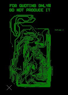
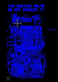
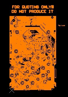
3G Wireless Router Printed Circuit Board Gerber Files:

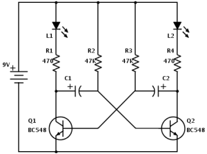
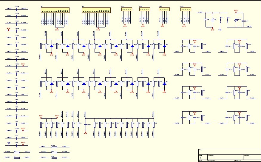
3G Wireless Router Printed Circuit Board Schematic Diagram:
Circuit Engineering Company Limited provide a complete PCB Reverse Engineering, PCB Clone and PCB Copy service, Rapid Prototyping and functional test services using the latest technologies combined with traditional skills for a wide range of industries. By integrating our traditional skills with the latest technologies, we can offer clients a comprehensive portfolio of product development services all under one roof. For more details please contact our customer
service team.
Tags: double side pcb recovery,gerber file recovery,pcb board recovery,pcba recovery,printed circuit board recovery,pwb recovery,schematic diagram recovery,wiring schematic recovery