

PCB Circuit Card Reverse Engineering Wave Simulation
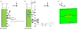
In this case, although the wave of simulation result from PCB circuit card reverse engineering could be integrated without any singularity, but in fact, if the signal singularity has come to the step of not working situation, so sometimes, engineer will ask this question: “why the signal wave has show no existence of change in the signal integrity no matter how thin we have layout the power supply tracks and grounding tracks in the process of Pcb circuit card reverse engineering?” that is because the signal integrity simulation hasn’t taken your power integrity into consideration.
PCB Circuit Card Reverse Engineering Wave Simulation
The only way to solve this problem is use SPI tools. SPI can take the ground power layer, include the ground power tracks inside the signal layer into account when proceed the signal integrity analysis as well as the large copper filling issue. However, these unstable signals or interference from ground power layer will be overlapped into the signal integrity simulation result.
Through which the real simulation result can be obtained, and of course the final result will be quite close to the real test result. In order to facilitate the engineer direct consideration and rectification in the process of Pcb circuit card reverse engineering, APSIM-SPI has come to realize the integration of SI AND PI organically, no matter from the internal model, algorithm, calculation and user interface, analysis functions and stimulation mechanism have all been modified dramatically, the RLGC parameter from SPI extraction could be much more complicate than simply extract from the SI parameter.
Since in the SPI, parasite parameters in the grounding power layer must be considered thoroughly when replicate pcb circuit card as well as the connection relationship between ground layer and signal layers.
Tags: reverse engineering electronic board artwork,reverse engineering electronic board bill of material,reverse engineering electronic board bom,reverse engineering electronic board cad file,reverse engineering electronic board design,reverse engineering electronic board gerber file,reverse engineering electronic board layout,reverse engineering electronic board schematic