

PCB Circuit Board Reverse Engineering
PCB Circuit Board Reverse Engineering is a process to extract the schematic diagram, gerber file and layout drawing, BOM list from original printed circuit board which can be used for re-produce the PCB card;
If we need to connect two PCB circuit board together, we will use use the golden finger also know as edge connector. There are a lot of exposed copper pad on the golden finger and they are actually also part of the PCB circuit board layout frame work.
When we connect the PCB board, the golden finger on one of the PCB card will be inserted into another printed circuit board with proper expansive slot.
In the personal computer, such as the video card, audio card or other interface card, all of these are need to use golden finger to connect the mainboard when reverse engineering printed circuit board.
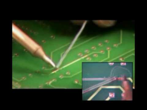
The green color and grey color on the PCB board reverse engineering is the color for the solder mask or solder resist. This is the protective layer for insulation, it can be used to protect the copper wire, it can also prevent the components being mounted onto other improper places.
On the protective soldering resist layer we will also print a silkscreen layer. Normally it will be printed the markings or legend and most of them are white, to signify the location of each components;
Tags: reverse engineering circuit board,reverse engineering circuit card,reverse engineering pcb,reverse engineering pcb assemble,reverse engineering pcb board,reverse engineering pcb card,reverse engineering pcba,reverse engineering printed circuit board,reverse engineering printed wiring board,reverse engineering pwb,reverse engineering pwba