

PCB Circuit Board Reverse Engineering Lines
The silkscreen layer from PCB Circuit Board Reverse Engineering is special because there are actually two silkscreen layers, one for the top (component) and one for the bottom (solder) side of the board. Which silk layer you draw on is determined by the side of the board that you are viewing. If you are viewing the component side, then drawing on the silk layer draws to the component-side silk layer.
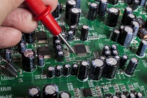
PCB Circuit Board Reverse Engineering
The netlist layer is another special layer. It shows rat’s-nest lines (i.e. guides that show how the netlist expects the element to interconnect). If you make this the active layer, you can use the Line tool to add entries into the netlist, or to delete connections from the netlist window.
Except for these two purposes, you should not make the netlist layer the active layer. Usually there is no need to do this because a separate schematic package should be used to create the netlist and for PCB design purpose. PCB Reverse Engineering decoupling can automatically draw all of the rats from the netlist. In some cases you may want to make a small change without going to the trouble of modifying the schematic, which is why this facility is provided.
Tags: pcb board reverse engineering,pcb card reverse engineering,pcb reverse engineering,pcba reverse engineering,Printed Circuit Board Reverse Engineering,printed wiring board reverse engineering,pwb reverse engineering,pwba reverse engineering