

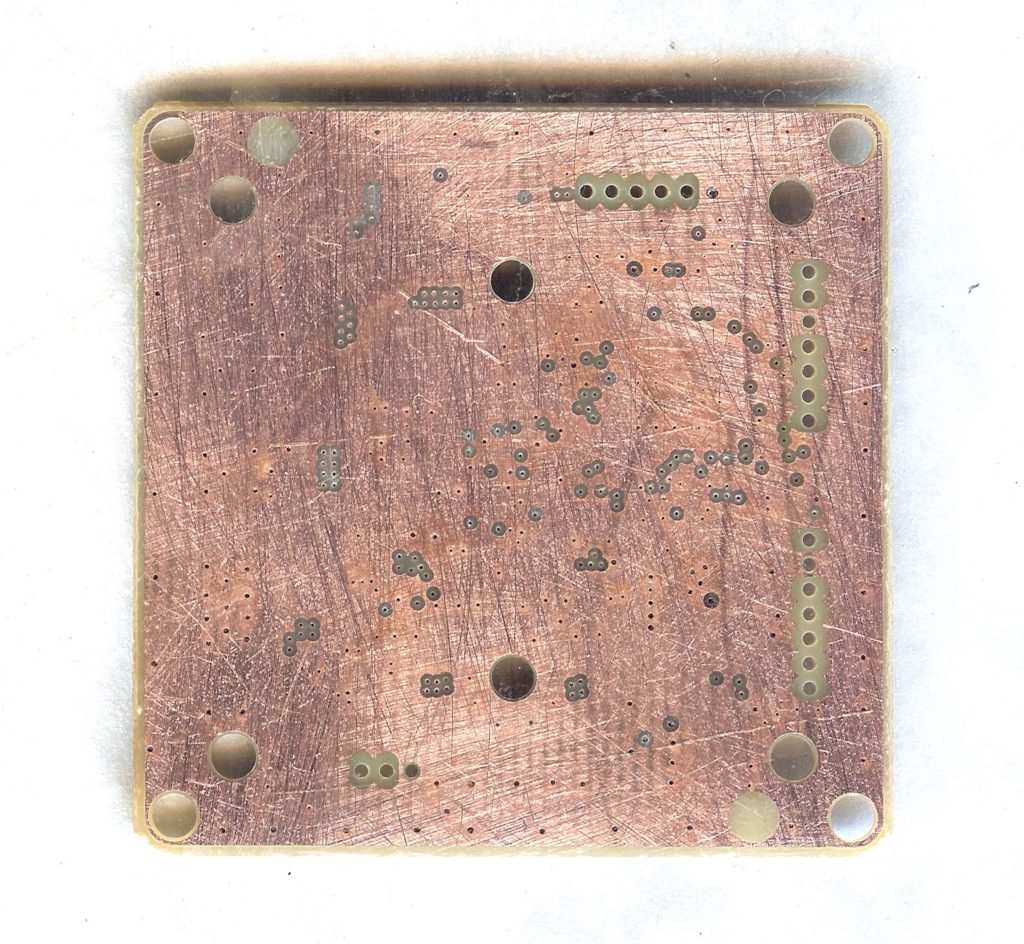
PCB Circuit Board Reverse Engineering Component Layout
PCB Circuit Board Reverse Engineering Component Layout can help to generate netlist of PCB card documents cloning and fulfill the task of netlist table analysis.
In the process of Circuit Board Reverse Engineering, for the sake of electronic component assemble optimum, design for manufacture rules will have some limitations upon the component layout. If the movement of electronic components is allowable in the pcb board assemble department, then it is feasible to make some optimization on it which can also facilitate the automatic layout. Hereby the defined rules and restriction terms can affect the layout design.
It is necessary to consider the routing channel and through hole area, these routes and area is quite obvious regarding to the PCB Reverse Engineering testing accuracy. However, the automatic layout tool will consider one signal each time, and it can complete the PCB Reverse Engineering job through the installation of layout restriction terms and layer where can layout the signal lines in compliance with the thoughts.
Tags: pcb assemble reverse engineering,pcb board reverse engineering,pcb card reverse engineering,pcb reverse engineering,pcba reverse engineering,Printed Circuit Board Reverse Engineering,printed wiring board reverse engineering,pwb reverse engineering,pwba reverse engineering