

PCB Card Reverse Engineering New Element
PCB Card Reverse Engineering New Element actually is concept used in the redesign printed circuit board layout, through replicating electronic PCB board design scheme and gerber file, schematic diagram, the file which reflect original circuit card can be restored and then modify its design.
When you create a new element, remember that silkscreen lines should never overlap the copper part of the pins or pads, as this can interfere with soldering. The silkscreen should identify the maximum extent of the element package so it is easy to see how close elements can be placed together.
If you want to make an element similar to an existing one, you can break an element into constituent pieces from the Buffer menu. Paste the pieces to the layout, make the necessary changes, then convert it back into an element.
If the pin numbers haven’t changed, there is no need to name each via/line as they are pre-named when the element was broken apart. When you create a new element, you can save it to a file in order to have easy access to it the next time you.
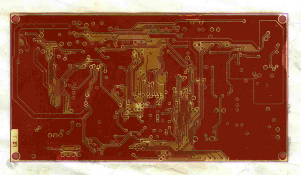
Every layout and schematic restored from electronic pcb board consists of several layers that can be used independently or treated as a group. Layer groups can be used to logically separate (and color-code) different traces (e.g. power and signal); however, all layers within a group reside on the same physical copper layer of a card, so using different layers within the same group won’t provide electrical separation where they touch or overlap. For details, see ‘layerGroups’, Section 6.1 [Resources], page 38. Each layer is drawn in a color defined in the resource file and identified by a name that you can change (for details see ‘layerColor’, Layers are really just containers for line, arc, polygon, and text objects.
The component and solder layers contain SMD elements as well, but the file structure doesn’t reflect that fact directly. Each layer group represents a physical layer on the printed circuit card. If you want to make a four layer card, you’ll need to have at least four layer groups.
Connections between layer groups are established only through element pins and vias. The relationship between a specific layer and the card itself is configurable from the ‘Edit layer groups’ option in the Settings menu. The layer groups corresponding to the physical layers: component-side and solder-side are always defined and you must map at least one logical layer to each, even if you plan to make a single-sided card. You are not obligated to put tracks on either of them.
Surface mount elements always reside on either the component-side or the solder-side layer group. When you paste an element from the buffer, it will go onto whichever side of the card you are viewing.
Tags: replicate pcb card artwork,replicate pcb card bom,replicate pcb card component list,replicate pcb card design,replicate pcb card diagram,replicate pcb card drawing,replicate pcb card gerber file,replicate pcb card layout,replicate pcb card part list,replicate pcb card schematic