

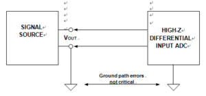
PCB Card Cloning Concept
An illustration of the PCB Card Cloning concept using an ADC with high impedance differential inputs is shown in below Figure.
A High-Impedance Differential Input ADC Also Allows High
Note that the general concept can be extended to virtually any signal source, driving any load. All loads, even single-ended ones, become differential-input by adding an appropriate differential input stage. The differential input can be
provided by either a fully developed high Z in-amp, or in many cases it can be a simple subtractor stage op amp.
Leakage resistance is the dominant static circuit board effect. Contamination of the PCB surface by flux residues, deposited salts, and other debris can create leakage paths between circuit nodes. Even on well-cleaned boards after PCB Card Cloning, it is not unusual to find 10 nA or more of leakage to nearby nodes from 15-volt supply rails.
Nanoamperes of leakage current into the wrong nodes often cause volts of error at a circuit’s output; for example, 10 nA into a 10 MΩ resistance causes 0.1 V of error. Unfortunately, the standard op amp pinout places the −VS supply pin next to the + input, which is often hoped to be at high impedance! To help identify nodes sensitive to the effects of leakage currents ask the simple question: If a spurious current of a few nanoamperes or more were injected into
this node, would it matter?