

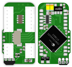
Mixed Signal PCB Board Partition
The two basic principles of electromagnetic compatibility (EMC) must be understood to help to faciliate the process of Mixed Signal PCB Board Partition:
How to reduce the mutual interference between digital signals and analog signals?
The two basic principles of electromagnetic compatibility (EMC) must be understood before reverse engineering PCB Board,
the first principle is to reduce the area of the current loop as much as possible;
The second principle is that the system uses only one reference plane. Conversely, if the system has two reference planes, it is possible to form a dipole antenna (note: the radiation size of the small dipole antenna is proportional to the length of the line, the magnitude of the current flowing, and the frequency);
Mixed Signal PCB Board Partition
and if the signal can’t pass as much as possible with a small loop return, it is possible to form a large loop antenna (Note: The size of the radiation of the small loop antenna is proportional to the loop area, the current flowing through the loop, and the square of the frequency). Avoid these two situations as much as possible.
It has been suggested to separate the digital ground and the analog ground on the Mixed Signal PCB Board to achieve isolation between the digital ground and the analog ground. Although this approach works, there are a number of potential problems that are particularly acute in complex large systems.
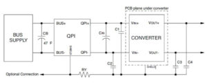
active filter control emi capability
The most critical issue is that it is not possible to route across the split gap when layout PCB diagram through reverse engineering. Once the split gap wiring is crossed, electromagnetic radiation and signal crosstalk increase dramatically. The most common problem in Mixed Signal PCB board partition is the EMI problem caused by the signal line crossing the split ground or the power supply.