

Ground Noise and Ground Loops
A more realistic model of a ground system from PCB Reverse Engineering is shown in below Figure. The signal return current flows in the complex impedance existing between ground points G1 and G2 as shown, giving rise to a voltage drop X V in this path. But it is important to note that additional external currents, such as IEXT, may also flow in this same path. It is critical to understand that such currents may generate uncorrelated noise voltages between G1 and G2 (dependent upon the current magnitude and relative ground impedance).
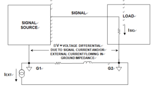
A More Realistic Source-to-Load Grounding System View Includes
Some portion of these undesired voltages may end up being seen at the signal’s load end, and they can have the potential to corrupt the signal being transmitted. It is evident, of course, that other currents can only flow in the ground impedance, if there is a current path for the circuitry acquired from PCB Reverse Engineering. In this case, severe problems can be caused by a high current circuit sharing an unlooped ground return with the signal source.
Below Figure shows just such a common ground path, shared by the signal source and a high current circuit, which draws a large and varying current from its supply. This current flows in the common ground return, causing an error voltage X V to be developed.
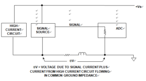
Any Current Flowing Through a Common Ground Impedance Can
From below Figure, it is also evident that if a ground network contains loops, or circular ground conductor patterns (with S1 closed), there is an even greater danger of it being vulnerable to EMFs induced by external magnetic fields. There is also a real danger of ground-current-related signals “escaping” from the high current areas, and causing noise in sensitive circuit regions elsewhere in the system.
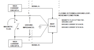
A Ground Loop