

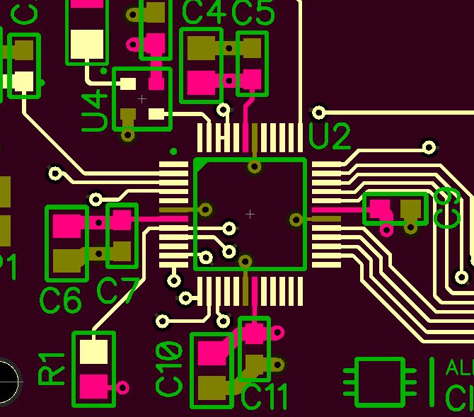
Electronic PCB Card Reverse Engineering Decoupling
Electronic PCB Card Reverse Engineering Decoupling conclusions can be drawn from these results. The main conclusion is that decoupling capacitors should be distributed across the entire board to help reduce the Electronic PCB Card resonances.
These board resonances are the main decoupling problem at high frequencies (above about 20 MHz). The actual resonant frequency will change as the number, or location, or value of decoupling capacitors is changed.
Predicting the exact resonant frequencies is impossible (given the number of variables), and so it must be expected that any harmonic noise will be at a frequency where a resonance occurs (worst case) before Electronic Printed wiring board clone defects.
Therefore, the individual S21 peaks are not as important as the overall envelope of the S21 measurements. Traditional values of capacitance (for example, .01 uF) make a significant improvement in the S21 at frequencies below about 200 MHz, but make only a little change at higher frequencies.
This is mostly due to the self resonance of the capacitor, and the inductive nature of the capacitor above its natural resonant frequency. Therefore, high frequency capacitors should also be distributed across the board. The value of these capacitors will determine the frequency range over which they are effective.
The majority of emissions from a two-plane structure is along the edge of the board. Care should be taken to ensure that no large openings in the shielded enclosure exist near the edge of the board.
The testing of these various configurations is very time consuming. Now that a good base of test data is available, this data should be used to validate a modeling technique, and then the models used to simulate the performance of various other decoupling configurations and all these datas can be optimized by PCB circuit board relayout.
One potential configuration that shows promise is to combine the resistor-capacitor edge termination with ‘regular’distributed decoupling capacitors. It is quite possible that this combined approach will allow the distributed capacitor approach to use less capacitors and thus same cost and space on the board.
Tags: pcb assemble reverse engineering,pcb board reverse engineering,pcb card reverse engineering,pcb reverse engineering,pcba reverse engineering,Printed Circuit Board Reverse Engineering,printed wiring board reverse engineering,pwb reverse engineering,pwba reverse engineering