

Electronic PCB Card Reverse Engineering Through Hole
Electronic PCB Card Reverse Engineering can extract the printed circuit board layout and schematic drawing which include the through hole design, if this technology can be applied on the double sided Electronic pcb card, then the drilling must go through this PCB board.
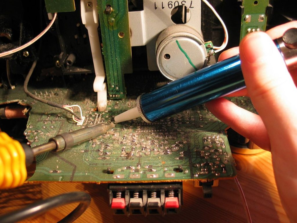
However, in the multilayer Electronic pcb board cloning, if you just want to electrically connect part of the wires, then these through holes could probably waste the space of several layers. Buried vias and blind vias technology can help you avoid the issues in this way, since they will go through only several layers of PCB board.
Blind vias can connect the internal layers with the layers on the surface, without go through the whole Electronic pcb card. buried via is in charge of get connected the internal layers so after the process is done, there is no way for you to see the vias. In the Electronic pcb card reverse engineering, the whole layer must be connected with grounding wire and power supply wires. So we have to separate them into signal layer, power layer or ground layer. If the components on the Electronic pcb card need to use different power supplies, reverse engineering Electronic pcb card will need to save more than 2 layers of power supply and wire layers.
Circuit Engineering Co.,Ltd. is a premier contract engineering service that provides global electronics manufacturing services which include the multilayer pcb board reverse engineering. We develop, manufacture, and ship and warrant products for our customers. These services increase customer competitiveness by delivering improved product quality, improved performance, and reduced costs.
Headquartered in Longhua district, shenzhen, we are an Electronics engineering and Manufacturing Services provider focused on delivering complete PCB Reverse Engineering and manufacturing services to automotive, gaming, consumer, medical, science education, and food processor OEMs. We develop, manufacture, and ship electronics products for our customers through facilities in Nevada and Mexico.
By combining development and engineering solutions with core electronics manufacturing services, we optimize our customers’ operations and lower their cost with domestic manufacturing and manufacturing in ASIA.
Tags: pcb assemble replicating,pcb board replicating,pcb card replicating,pcb replicating,pcba replicating,printed circuit board replicating,printed wiring board replicating,pwb replicating,pwba replicating