

Electronic PCB Card Cloning Capacitance
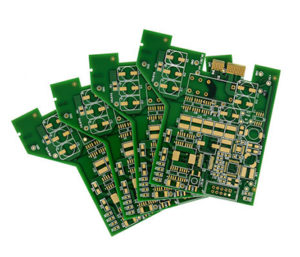
Electronic PCB Card Cloning Capacitance
Electronic PCB card cloning will cover the low frequency range, big capacitor will provide the low resistance grounding. Once the frequency can achieve their resonance value, the capacitance of the capacitor will decrease and gradually show the inductance. That is also the reason why the designers have to apply more than one capacitors on the circuitry: when one of the capacitors’ frequency is start to decreasing, the other capacitor’s frequency radiation can take into effect which makes it possible to keep the relatively low Alternative current resistance within the ten times of radio frequency range.
Start directly from the power supply lead of the algorithm amplifier when electronic pcb card cloning; the capacitors with the minimum capacitance value and the minimum physical size should be placed on the same side of the electronic pcb card. and it is better to close the amplifier as much as possible. The grounding terminal of the capacitor should use the shortest lead or the circuits should connect to the ground layer directly when electronic pcb card cloning. And the grounding connection described above should close to the amplifier’s negative terminal as much as possible to reduce the interference among the power supply terminal and grounding terminal after electronic pcb card cloning.
Refers to the electronic pcb card cloning, as for the capacitor with second large capacitance should repeat this process, so the designer it is better to place the capacitor from the smallest one and place a 2.2nf electro capacitor with identical series resistor effect. Apply 0508 enclosure dimension with 0.01nf capacitor with extremely low series inductance and excellent high radio frequency performance when electronic pcb card cloning.
From the power supply terminal to another power supply terminal, use another configuration way: apply one or more sideroad capacitors to cross the positive power supply terminal and negative power supply terminal. This is the method which will be applied only when designer feel difficult to install four capacitor in the tracks when electronic pcb card cloning. Its drawback is the enclosure size of the capacitor could increase since the voltage on the two side of the capacitor could be twice of the voltage in the single power supply sideroad system.
Increase the voltage will require to enhance the default breakdown voltage in the capacitor which means the size of the enclosure must be increased. However, this method can improve the PSR and performance lost functionality. Since the various circuits and layouts are all different, so the installation, quantity and capacitor value of the system will be determined according to the actual tracks when electronic pcb card cloning.