

Electronic PCB Board Reverse Engineering Service
In order to provide a better result for Electronic PCB Board Reverse Engineering Service, the try to make the distance between the hole distance and other components as much as possible, and standardize its dimension and optimize the processing through automatic insertion machine; don’t plating the fixed hole, since the radius of fixed plated hole could be quite difficult to control; engineer can try to make the fixed hole become the assemble hole when the final stage of reproduction of pcb board come, which can help to decrease the drilling hole process;
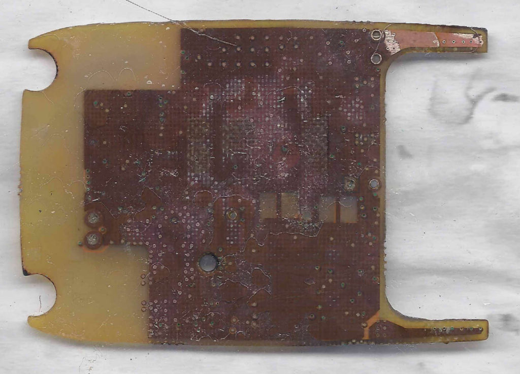
7; arrange the testing schematic diagram near by the scraped side of circuit board for the convenience of technology control; in the process of Electronic pcb board manufacturing, can use the same schematic diagram obtain from the circuit board restoration service to proceed the resistance value, impedance control, cleanliness and solderability, etc.
8; As for those bigger size Electronic pcb board, should leave a path in the center of it which can provide mechanical support on the Electronic pcb board when wave soldering, it can great prevent the Electronic pcb board droop and soldering tin sputtering and make the soldering consistently;
9; considering the nail bed detectable issue when copy pcb board gerber file, can use surface soldering pad without lead to facilitate the on-site test and make all of the electrical nodes are all detectable;
Tags: pcb assemble duplicate,pcb board duplicate,pcb card duplicate,pcb duplicate,pcba duplicate,printed circuit board duplicate,printed wiring board duplicate,pwb duplicate,pwba duplicate