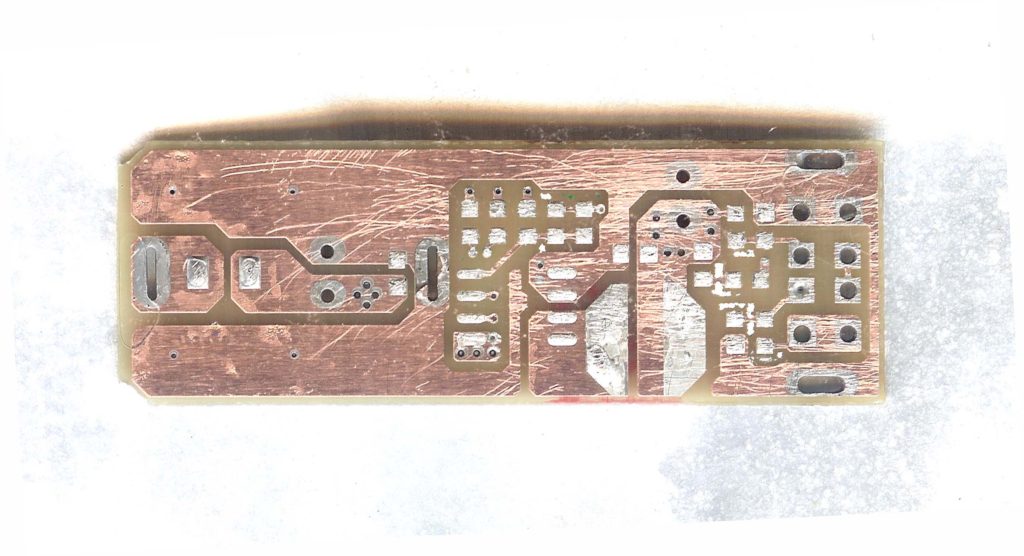
Electronic PCB Board Reverse Engineering Introduction
Electronic PCB Board Reverse Engineering is a industry which requires sufficient experience, circuit engineering co.,ltd has been in this industry for years and have accumulated lots of experiences.

We have seen Electronic PCB Boards from over several hundreds of different products in various industries, such as air conditioning, Liquid Crystal Diode TV, digital photograph frame, and other automatic industry products, etc. in view of a printed electronic pcb board reverse engineering engineers, some of these Electronic pcb Boards have good design features, some others not. The only standard for design a good Electronic pcb Board is whether it can be checked and viewed by engineers from manufacturing factory clearly and effortlessly, without any misunderstanding which can cause the wrong operation and production.
When deign the track pattern on the pcb board technology reverse engineering, we will encounter the line width and space, as well as open and short electronic pcb issues, etc. it is the most commonly see things, for some electronic pcb board with regular requirements, the track width and space should be as wide as possible; also there are some electronic pcb board layout file,
On which with some tracks parallel to each other, while part of which space is 0.1mm and other is 0.2mm space, so when reverse engineering pcb board design, engineers should pay attention to these issues, sometimes the distance between a electronic pcb and copper foil is only 0.127mm after reverse engineering electronic pcb board which has greatly increase the difficulty on taking care of film when manufacture electronic pcb board, we should ensure the least distance between a electronic pcb and copper area is 0.25mm or above.
As we might know, some of the electronic pcb board track pattern has very little secure distance between profile or V-CUT area, some of them can be removed by manufacturer, but some of them can only be moved by engineers who operate the circuit board reverse engineering. Even sometimes the electronic pcb tracks have been connected together from different networks after printed circuit board reverse engineering, and sometimes the electronic pcb pattern didn’t connect each other even if they are actually from the same network, and finally the manufacturer has to communicate with design engineers, and found its actually a open/short electronic pcb which require to modify the layout.
We have found a lot of similar cases which count not the less part, some of the veteran engineers who do PCB card cloning for years could probably figure it out, but some of the electronic pcb board reverse engineer can only follow the original layout and file to proceed the process, and the final consequence is modify the original files or use knife to cut off the short electronic pcb.
As for the electronic pcb board with impedance control requirement, due to the lack of proper description, it finally fail to meet the expectation, and some of the drill holes have been designed on the SMD PAD which will cause the solder tin leaking when assemble electronic pcb board.
Tags: cloning pcba,cloning printed circuit board,cloning printed wiring board,cloning pwb,cloning pwba

