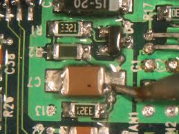
Cloning Printed Circuit Board Component Layout
Cloning Printed Circuit Board Component Layout which include all the information of each electronic parts, and specification through which the PCB board can be assembled and populated properly after PCB card cloning;

A well performed device, except the high quality component selection, reasonable Printed circuit board layout, optimized components layout and preferred structure design in the electrical/electronic orientation can determine if the device can work in a reliable situation.
As for the Printed circuit board with same components and parameters, the functionality result could be quite difference due to the different combination and arrangement of component layout design and electrical orientation. As a result of that, it is quite necessary to take the correct Printed circuit board layout optimization, circuit tracks orientation and mechanic structure of instrument into consideration. Since a reasonable mechanical structure, can not only eliminate the noise interference generated from the inappropriate layout, but also bring great convenience for the assembly, debugging and maintenance, etc.
Since there is no limitation and definition for the good structure, so each one of the instruments must constructed by electrical functionality, whole set structure installation and panel layout to apply the corresponding layout design solution in the process of Printed circuit board reverse engineering, and prepare several selectable options for comparison and modification.
Tags: cloning pcba,cloning printed circuit board,cloning printed wiring board,cloning pwb,cloning pwba

