

Cloning PCB Card
Most of the engineers will consider the layout of each layer when Cloning PCB card, and often be confused by whether the signal layer or groundling layer should be Cloning and if the signal layer and groundling layer should placed in turns or in a concentrated place. Now, the engineer can clearly understand which way is better by the assistance of SPI simulation result.
For example, when there are multiple power supply sources on the ground line layer, such as 3.3V ground, 2.5V ground, 5V ground, how to separate them in reason? In the past, engineer will Cloning PCB Card only according to their experience and can only conside the possibility and rationality only through the border separation. If this aspect can’t be solved properly will cause a worse result which the engineers all have the deep experience.
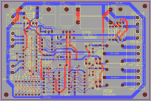
However, since the ground layer is normally in the midst of PCB Card, so it can’t be contact physically and it is difficult to proceed any debugging or modification. As a matter of fact, when proceed the multiple source power supply design, not only the border issue must be considered in different zones, but also the wave filtering issue, common ground issues, etc. once the existence of SPI tool, engineer can instruct the multiple power supply separation rationally with great convenience since the simulation signal will distort once the the layout process is not good.
Circuit Engineering Co.,Ltd. is a leading provider of PCB Card engineering and manufacturing services incorporating design/reverse engineering, PCB assembly, box build, global supply chain management and integrated technologies.
With specialist knowledge of integrated design and manufacturing solutions for high technology, high mix and complex products, we offer a complete service from PCB reverse engineering/design (electronic, mechanical and software), prototype, new product introduction (NPI), global procurement, in house tooling and moulding, PCB assembly, box build and test, packaging and global logistics.
Our design and engineering expertise – from product design based on customer concept through to re-engineering of existing assemblies – provides comprehensive design support throughout your product life cycle.
With a choice of manufacturing location to suit your volume and technology requirements, we provide global procurement and cost effective sourcing through wholly owned facilities in the Asia.
As a strategic design and manufacturing partner, we provide a complete end-to-end managed solution delivering your product on time and on budget.