

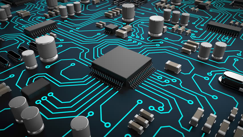
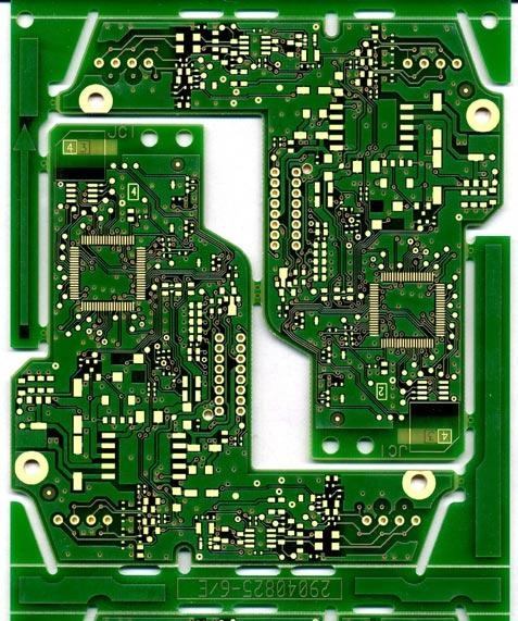
Cloning PCB Card Process
In order to solve the signal integrity issue in the process of cloning pcb card process, design engineers will invest more time and energy into the restriction terms and definition stage for Pcb card Cloning. through the signal analysis tools developed in the early stage of cloning, use multiple simulation, and carefully plan the circuit board topology structure, it will construct the electrical features and physical features’s comprehensive restricted terms to avoid the issue mentioned above:
In the process of Pcb card cloning, there is no design environment can fully adapted to the new design requirement, and the current typical design environment are all face with the later part of Pcb card cloning, and will always take the PCB drawing as main consideration effect.
and the tool providers are all start to engage in these new challenges. but the design engineers need to fully new way to solve the high speed design issue which they will encounter in the process of Pcb card cloning each day. use the methods mentioned below can help to solve some of the problem emerge in the early stage:
Use the more dense tool integration
When Pcb card cloning, in order to find out and tackle the high speed issue when cloning pcb card without rely on the expensive and time consuming pcb card test procedures, it is critical to proceed great amount of the signal analysis. the reason for doing so it is because once these issues can be spotted by the design engineers, it can ensure the first yield rate of pcb card Cloning through change the layout, layer distribution, clock wire definition and layout topology, choose the components with specified speed.
Tags: copy small controller board artwork,copy small controller board bom,copy small controller board cad file,copy small controller board design,copy small controller board gerber file,copy small controller board layout,copy small controller board schematic