

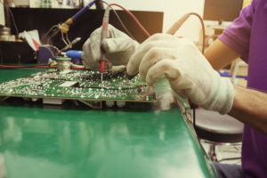
Anti-ESD Design in Reverse Engineering PCB board
Anti-ESD Design in Reverse Engineering PCB board can be realized by layering, proper layout and installation. By adjusting the PCB layout and wiring, ESD can be well protected. Multilayer PCBs can be used as much as possible.
Compared to double-sided PCBs, ground planes and power planes, as well as closely spaced signal line-ground spacing can reduce common mode impedance. It is inductively coupled to 1/10 to 1/100 of a double-sided PCB. It has components for the top and bottom surfaces and has a short connecting line.
Static electricity from inside the human body, the environment, and even electronic equipment can cause various damage to delicate semiconductor chips, such as penetrating a thin insulating layer inside the component; damaging the gates of MOSFETs and CMOS components; and flip-flops in CMOS devices Short-circuited, reverse-biased PN junction; short-circuited forward-biased PN junction; melted weld line or aluminum wire inside the active device.
In order to eliminate the interference and damage of electronic devices caused by electrostatic discharge (ESD), various technical means are needed to prevent them.
Anti-ESD Design in Reverse Engineering PCB board
Anti-ESD Design in Reverse Engineering PCB board can be realized by layering, proper layout and installation. In the design process, most of the design modifications can be limited to increasing or decreasing components through prediction. ESD can be well protected by adjusting the PCB layout. Here are some common precautions.
When using a multi-layer PCB as much as possible, the ground plane and power plane, as well as the closely spaced signal line-ground spacing, can reduce common mode impedance and inductive coupling relative to a double-sided PCB, enabling it to reach 1/2 of a double-sided PCB. 10 to 1/100. Try to keep each signal layer close to a power or ground plane. For high-density PCBs with components on the top and bottom surfaces, short traces, and many fill locations, consider using inner traces.